Table of Contents
DS Linker Writer/N-Card (Slot-2 USB cart)
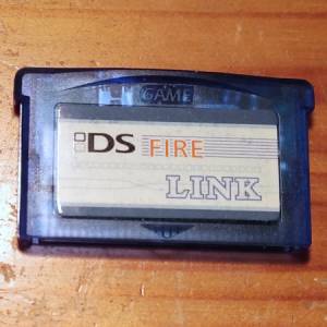
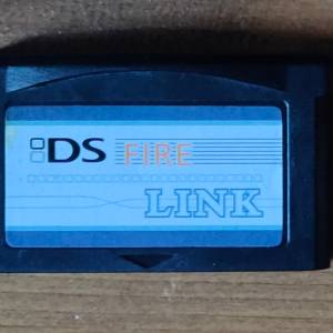
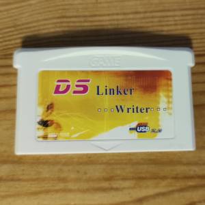
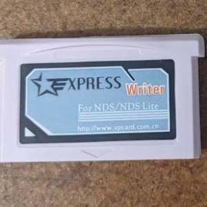
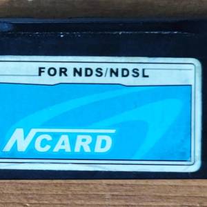
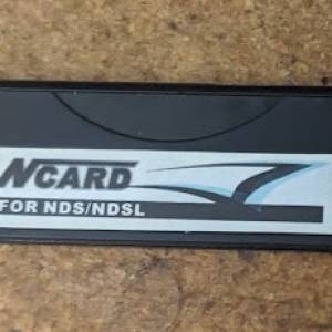
The DS Linker Writer (also known as the N-Card, ExpressCard, DS Fire Link, etc.) is a Slot-2 GBA cartridge with an USB controller; in combination with a software USB stack running on the DS itself, it allows the console to act as an USB device.
Two variants exist:
- the “D12”, featuring USB 1.1 support, based on a PDIUSBD12 chip.
- This chip was only used in early batches of the card.
- Due to a regression bug, this variant only works with older releases of uDisk. It also doesn't support homebrew built with the open source Keil stack.
- the “D14”, featuring USB 2.0 support, based on an ISP1581 (or equivalent) chip.
- The most common variant.
To identify the variant in your possesion, you can use nrio-usb-disk (linked below), which displays the detected chip ID:
1012- “D12” board (PDIUSBD12-based)1581- “D14” board (ISP1581-based)- other values - unknown chip
- The TinyUSB stack used by nrio-usb-disk can support
1582and1583boards (ISP1582/83-based), if any such turn out to exist.
0000,FFFF- unknown board (or no board!)
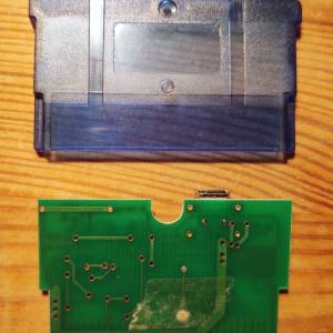
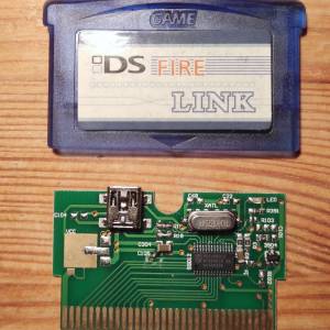
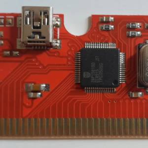
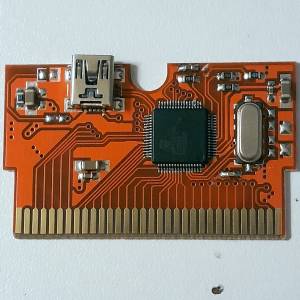
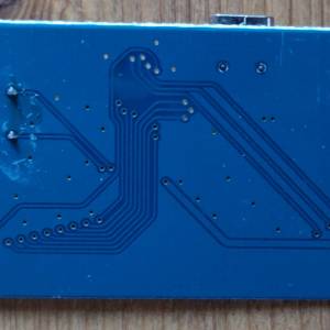
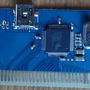
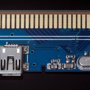
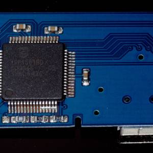
Alternatively, you can compare the PCB with photos available below.
Software
- NitrousTracker - music tracker, supports USB MIDI in versions 0.4.11+
- nrio-usb-disk - USB mass storage driver, compatible with any Slot-1 DLDI flashcart
- DSMouse - mouse emulator
- DSPad - gamepad emulator
- DSPad Tilt - gamepad emulator with motion controls (DSMotion/MK6/R6 required in Slot-1)
- uDisk - official USB mass storage driver, supports N-Card only
Implementations
- TinyUSB port - MIT licensed
- Requires a recent version of BlocksDS; comes with examples.
- Full support for “D14” and “D12” boards.
- Keil USB stack port by the N-Card/DS Linker team
- Contains examples intended for an ancient version of devkitARM/libnds.
- Full support for “D14” boards.
- No support for “D12” boards.
Photos
Cartridges
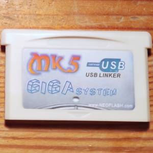
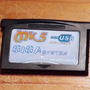
Note that the casing color may differ between batches.
D12
D14
(Source: ApacheThunder, Disturbo)
Notes:
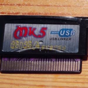
- The MK5 GIGA with a purple PCB and exposed pins is the only one on this list not to feature a mini-USB connector; rather, a non-USB-standard connector is used.
PCBs
DS Fire Link (D12)
DS Fire Link (D14)
ExpressCard Writer (D14)
N-Card (D14)
DS Link? (D14, "Lite" form factor)
Wiring
D14 (ISP1581)
The DS Linker Writer uses an ISP1581 (or clone, depending on batch) USB controller and a 12 MHz crystal.
In theory, it should be possible to replace the chip with an ISP1582 or ISP1583 in newer designs while maintaining compatibility.
TODO: Mark power pin connections?
                                  _____
                                 /     \
                           DGND / 1  64 \ VCC(3.3)
                      VCC(5.0) / 2 _  63 \ TEST
                         AGND / 3 / \  62 \ WAKEUP
                   VCCA(3.3) / 4  \_/   61 \ DGND
               USB D- <> D- / 5          60 \ XTAL1 <- 12 MHz oscillator
              USB D+ <> D+ / 6            59 \ XTAL2 -> 12 MHz oscillator
                      RPU / 7              58 \ VCC(3.3)
                    RREF / 8                57 \ DATA15 <> GBA AD15
                  MODE1 / 9                  56 \ DATA14 <> GBA AD14
                /RESET / 10                   55 \ DATA13 <> GBA AD13
                  EOT / 11                     54 \ DATA12 <> GBA AD12
                DREQ / 12                       53 \ DATA11 <> GBA AD11
               DACK / 13                         52 \ DATA10 <> GBA AD10
              DIOR / 14                           51 \ DATA9 <> GBA AD9
             DIOW / 15                             50 \ DATA8 <> GBA AD8
           INTRQ / 16                               49 \ DATA7 <> GBA AD7
                /                                       \
                \          Philips/NXP ISP1581          /
            /CS1 \ 17                               48 / DATA6 <> GBA AD6
             /CS0 \ 18                             47 / DATA5 <> GBA AD5
               DA0 \ 19                           46 / DATA4 <> GBA AD4
                DA1 \ 20                         45 / DATA3 <> GBA AD3
                 DA2 \ 21                       44 / DATA2 <> GBA AD2
                READY \ 22                     43 / VCC(3.3)
                  DGND \ 23                   42 / DGND
               VCC(3.3) \ 24                 41 / DATA1 <> GBA AD1
           GBA /CS <-/CS \ 25               40 / DATA0 <> GBA AD0
           GBA /RD <- /RD \ 26             39 / AD7 <- GBA A23
            GBA /WR <- /WR \ 27           38 / AD6 <- GBA A22
           GBA /IREQ <- INT \ 28         37 / VCC(3.3)
                          A0 \ 29       36 / DGND
               GBA A16 -> AD0 \ 30     35 / AD5 <- GBA A21
                GBA A17 -> AD1 \ 31   34 / AD4 <- GBA A20
                 GBA A18 -> AD2 \ 32 33 / AD3 <- GBA A19
                                 \     /
                                  \   /
                                   \ /
                                    V

                            GBA cartridge port

                    |________________________________|
                    |:                              :|
                    |::::::::::::::::::::::::::::::::|
                  1 |::::::::::::::::::::::::::::::::| 32
                     |||||||||||||||||||||||||||||||'- /GND
                     ||||||||||||||||||||||||||||||'- /IREQ
                     |||||||||||||||||||||||||||||'- /CS2
                     |||||||||||||||||||||'+++++++- A16-23
                     |||||||||||||||||||||
                     |||||'+++++++++++++++- AD0-15
                     ||||'- /CS
                     |||'- /RD
                     ||'- /WR
                     |'- PHI
                     '- VDD
D12 (PDIUSBD12) variant
A much rarer, alternate design uses a PDIUSBD12 chip instead, configured with a separate address/data bus.
In theory, it should be possible to replace the chip with an FT120, a modern replacement chip, while maintaining compatibility. However, minor differences exist, and this has not been tested on actual hardware.
TODO: Mark power pin connections?
                        /\
                       /  \
                      /    \
                      :  28 \ A0 <- GBA A16?
                    _./   27 \ VOUT(3.3)
                   /       26 \ D+ <> USB D+
                  /  o      25 \ D- <> USB D-
 GBA AD0 <> DATA0 \ 1        24 \ VDD
  GBA AD1 <> DATA1 \ 2    P   23 \ XTAL2 -> 12 MHz oscillator
   GBA AD2 <> DATA2 \ 3    D   22 \ XTAL1 <- 12 MHz oscillator
    GBA AD3 <> DATA3 \ 4    I   21 \ GL_N -> LED
           GND -- GND \ 5    U   20 \ /RESET <- GBA AD8?
      GBA AD4 <> DATA4 \ 6    S   19 \ /EOT
       GBA AD5 <> DATA5 \ 7    B   18 \ /DMACK
        GBA AD6 <> DATA6 \ 8    D   17 \ DMREQ
         GBA AD7 <> DATA7 \ 9    1   16 \ /WR <- GBA /WR
                GND -- ALE \ 10   2   15 \ /RD <- GBA /RD
             GBA /CS -> /CS \ 11         /
                     SUSPEND \ 12       /
                       CLKOUT \ 13     /
             GBA /IREQ <- /INT \ 14   /
                                \    /
                                 \  /
                                  \/
